Research Overview
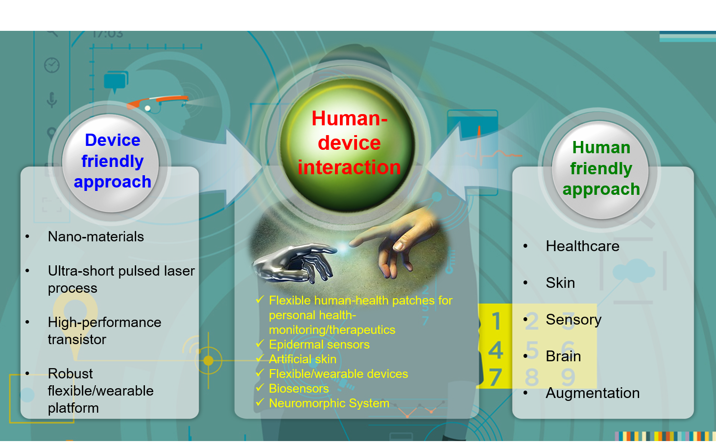
We cannot imagine that people can live without electrical devices. Therefore, interaction and interconnection between humans and devices are becoming more and more important with the lapse of time. The development of flexible electronics could be one reason because it is easy-to-read, lightweight, portable, flexible, and unbreakable. Given its attractive characteristics, nowadays, innovative flexible electronics are opening up next-generation technologies and leading the paradigm shift of electronic applications; potential applications could include flexible human-health patches, epidermal sensors, artificial skin, and electronic papers. It could change a picture of our life, which does not exist today. As science/engineering advances, we might all have the opportunity to see our dreams become a reality.
To ride the wave of the new industrial revolution, we will use a synergistic combination of 1) device friendly and 2) human friendly approaches as summarized in the below conceptual schematics.
Research Interests
– Flexible and wearable electronics and applications
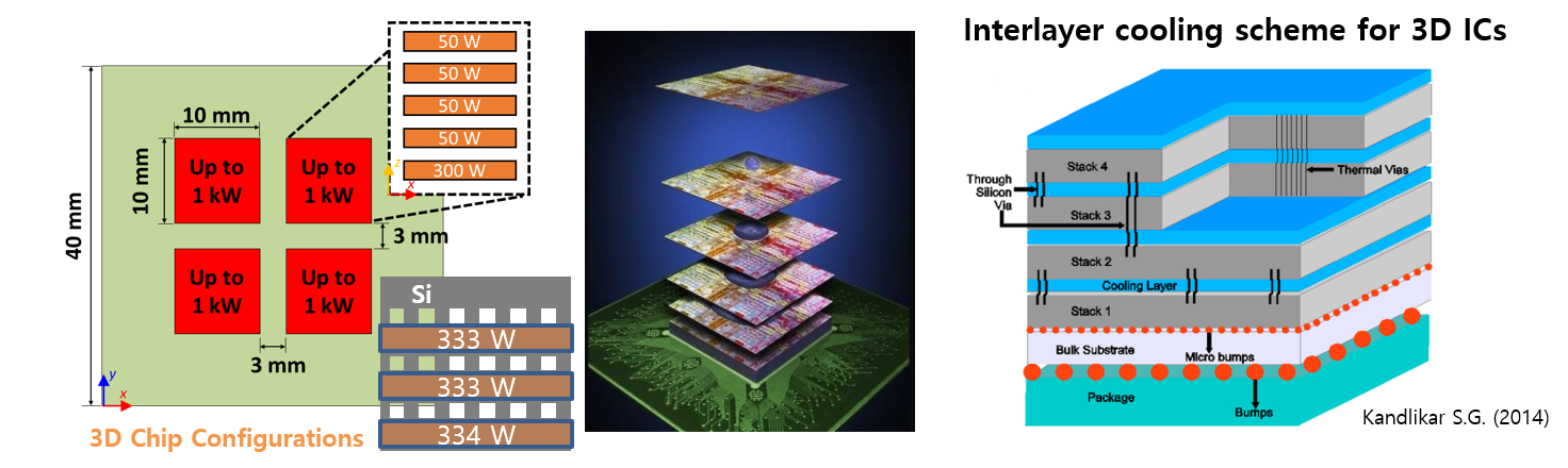
– Semiconductor fabrication technology for next generation monolithic 3D (M3D) architectures
– Device physics for semiconductor devices
– Site-selective laser processing
– Low-dimensional nano-materials
– Olfactory mimicking sensor and standardization of olfactory factors
– Micro/Nanoscale thermal/heat analysis
– Polymer like hyperelastic non-linear behavior analysis for stretchable and flexible form factor
– Solution processed low-cost printing technologies and development
– 3D hierarchical mechanical meta-structure and system
Next Generation Semiconductor Process for <3nm Technology Node
- Development of fabrication processes of a Gate-All-Around (GAA) structure with nanoscale analyses
- Established ultra-thin gate stacks for the GAA structure for <3nm tech node
- Study on barrierless contact metals for improving contact resistance
*Research project & funding source:
“Gate-all-around (GAA) Nanosheet structure for <3nm technology node," the Industry-University cooperation research grants funded by SEMES.
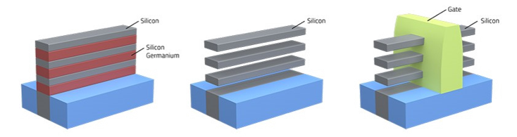
Low Temperature Process for Monolithic 3D (M3D) Architecture
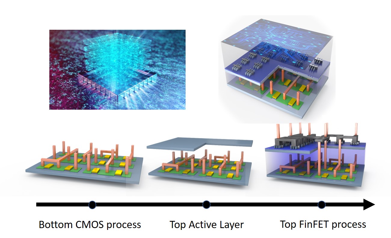
- Development of upper active layer process without thermal damage to the lower architecture
- Established a platform for fabricating upper tall FinFET devices based on a low temperature process
- Wafer-level M3D integrated Si(Ge) devices and circuits technology development
*Research project & funding source:
“Low temperature process of high crystalline Si(Ge) active layer for M3D integration," the National Research Foundation of Korea (NRF) grants funded by the Ministry of Science and ICT (MSIT).
Front-end-of-line (FEOL) Integration Platform for Extreme Low Power Device
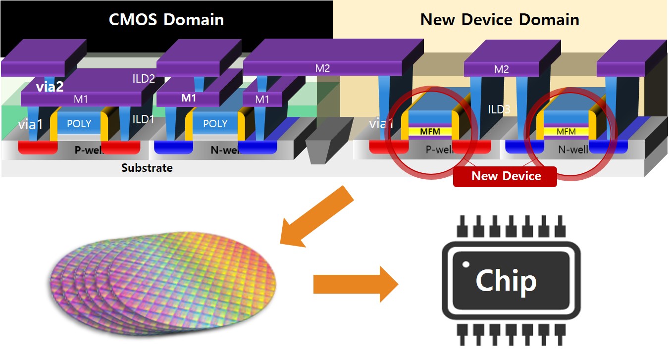
- Development of CMOS/New device (FeFET, NCFET, etc.) simultaneous integration platform
- Chip implementation for performance verification
- Wafer-level (6-inch, 8-inch) integrated new device and verification system
*Research project & funding source:
“Development of FEOL integration platform for extreme low power device," the National Research Foundation of Korea (NRF) grants funded by the Ministry of Science and ICT (MSIT).
Next Generation Display Driven by High Mobility 2D Semiconductor for Smart Mobility
- Development of rollable OLED manufacturing technology based on 2D semiconductor
- Recrystallization technology of high-crystalline Mo seed for large-area growth of 2D semiconductor
- Application to next-generation mobility information panel and CID (Center Information Display)
*Research project & funding source:
“Development of high-crystalline Mo seed for large-area growth of 2D semiconductor," the National Research Foundation of Korea (NRF) grants funded by the Ministry of Science and ICT (MSIT).
Convergence Research Advanced Centre for Olfaction (CRCO)
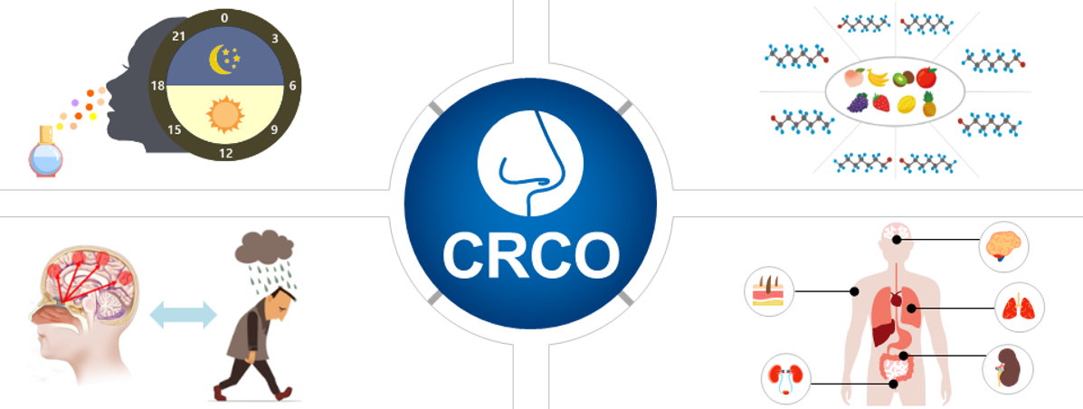
- Nurturing professional in olfactory field
- Understanding the olfactory nervous system
- Developing technology to olfactory sensors and standardization
*Research project & funding source:
“Convergence Research Advanced Centre for Olfaction," National Research Foundation of Korea (NRF) funded by the Ministry of Education.
Improvement of Electrical Interconnect and Contact
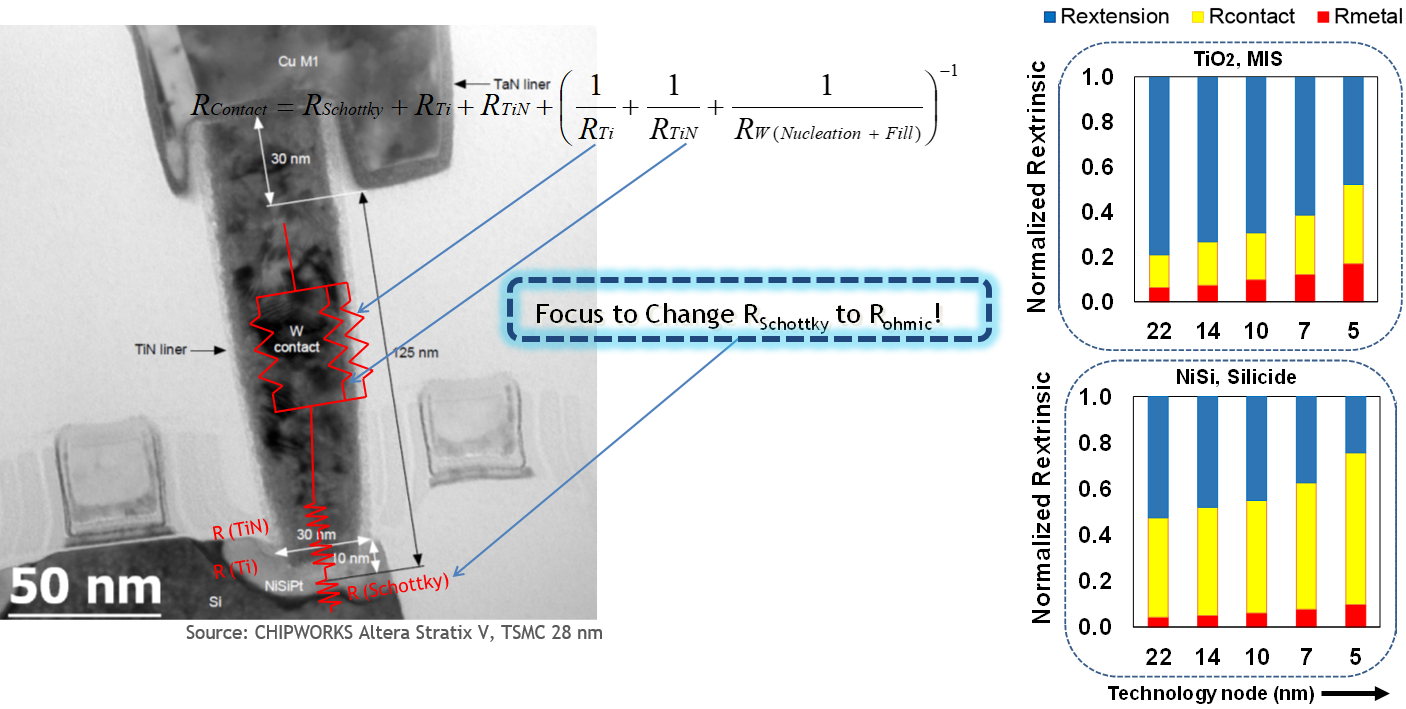
- Contact area goes down with scaling.
- As device scaling continues, parasitic source resistance largely dominated by contact resistance, is beginning to limit the device performance.
- We are developing Ohmic contact technology and improving metal interconnect for future electronics.
*Research project & funding source:
Funded by the Samsung Electronics & University R&D program
Development of Artificial Intelligence (AI) Based Exobrain System: Neural Network Devices
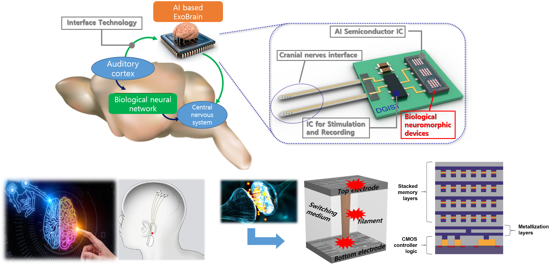
- Study on biological structure of neurons and synapses
- Understanding biological inspired architecture and system of neural network
- Development of hybrid neuromorphic systems
*Research project & funding source:
“Artificial intelligence based micro-miniature Exobrain," the National Research Foundation of Korea (NRF) grants funded by the DGIST R&D Program, Pre-Center of Excellence (P-CoE).
Intense Light Process with Nano-Materials
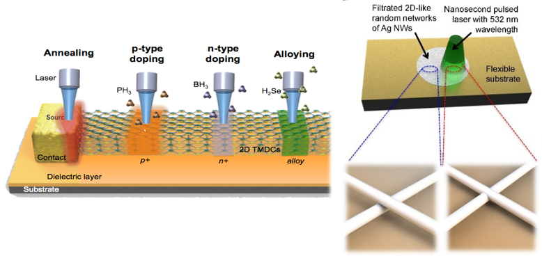
- Pulsed laser momentarily induces high temperature, imparting a smaller heat-affected zone.
- Laser processing can induce thermal effect at very locally confined small area that needs high temperature without incurring extreme thermal damage to surrounding regions.
- For nanoscale devices using nano-materials, the site-selective process enables achievement of superb electrical characteristics through annealing, doping, alloying, and welding.
*Research project & funding source:
“Intense optical pulse for the nano-scale surface modification and applications of the next generation electronic devices," the National Research Foundation of Korea (NRF) grants funded by the Ministry of Science and ICT (MSIT)
Programmable Digital Oxidation
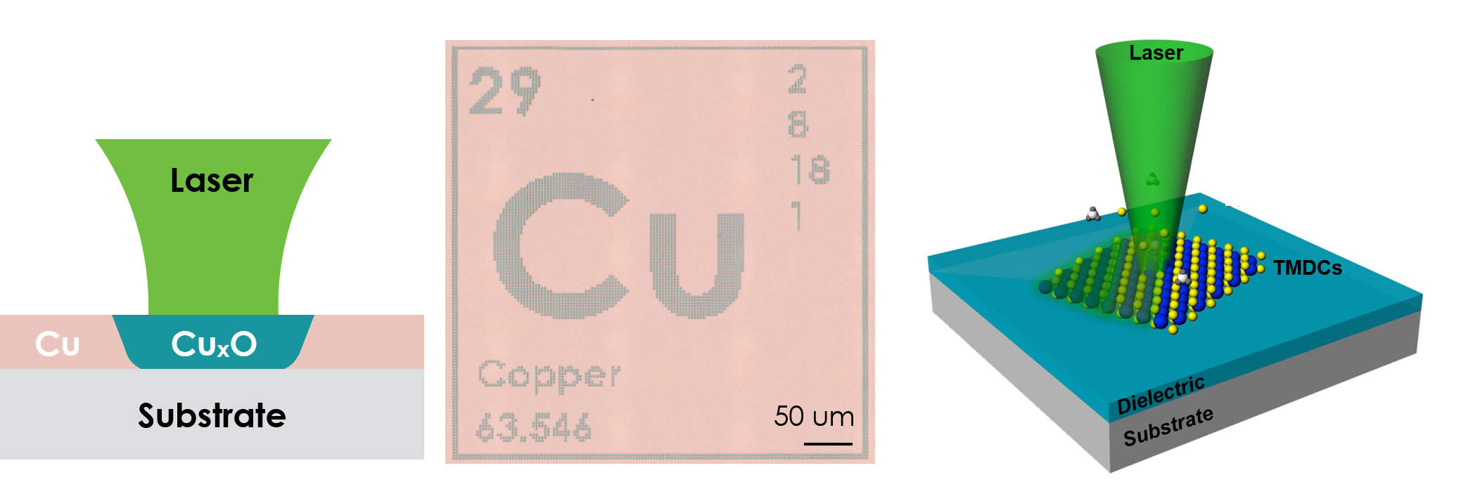
- With spatially controlled heating, arbitrary copper oxide semiconductor pattern can be monolithically written in copper film.
- Spatially controlled heating can be a facile manufacturing method to fabricate metal/semiconductor/metal (MSM) homo-junction structures.
- Horizontal band-gap tuned tandem structure can be realized by laser.
*Research project & funding source:
“A study on a laser nano-scale surface process," funded by Samsung Electronics
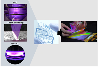
Robust Flexible/Wearable Platform
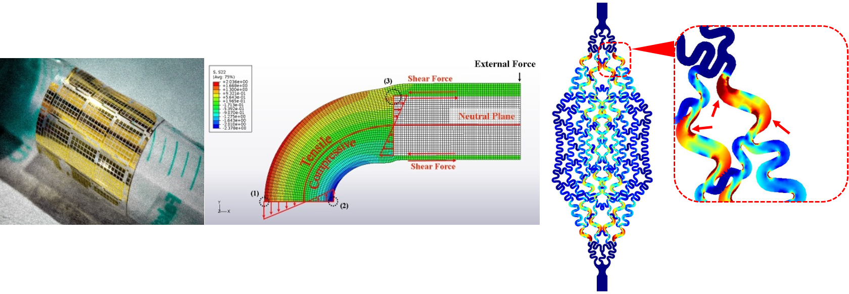
- Nature inspired sensor electrode design can achieve high-levels of deformability and stretchability.
- Finite element method (FEM) allows us to understand mechanical behaviors of the of nonlinear hyperelastic material and its structure.
- Through the real mechanical tests and analyses, we can fabricate robustly designed flexible/wearable platform.
*Research project & funding source:
DGIST Start-up Fund Program of the Ministry of Science, ICT (MSIT) and Future Planning
Human Augmentation System
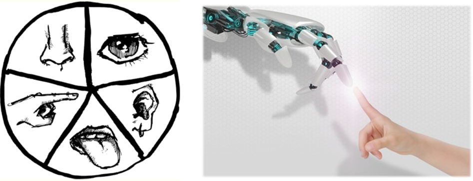
- The natural, artificial, or technological alteration of the human body enhances physical or mental capabilities.
- Bio-mimetic five sensory system is an important to the interface between human and machine.
- We need to understand and study on biological sensory mechanism and structure.
*Research project & funding source:
“Development of artificial sensors based on the mimic of human sensory system," the National Research Foundation of Korea (NRF) funded by the Ministry of Science and ICT (MSIT)
Si-based 3D Embedded Channel System for Power Semiconductors
- Utilizing embedded cooling can eliminate most of the thermal issues as it directly cools the GaN device closest to the heat sources.
- Fabrication of designed channels that can create direct jet impingement of the flow.
- Cooling down high heat flux devices through 3D embedded channels.
*Research project & funding source:
“Fabrication of Si-based embedded cooling channel for GaN device," funded by the Agency for Defense Development (ADD) & ATSLA Lab. at Chung-Ang Univerisity.
Research Sponsors