Previous Research Topics
Prof. Kwon had extensively worked on Next-generation displays & Semiconductor processes, Laser process, Disruptive electronic devices, and Flexible electronics. The following topics are selected research experiences and expertise.
2019.09~2022.08
AEDRG/K-Lab.,
DGIST, Daegu, S. Korea
Assistant/Associate Professor
*Funded by Samsung Science & Technology Foundation, S. Korea

3D Embedded Channel System for Semiconductor Devices with High Heating Value
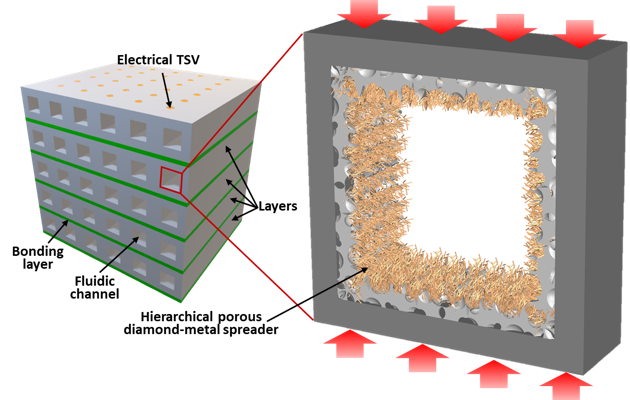
- Utilizing embedded cooling can eliminate most of thermal issues as it directly cools the semiconductor device closest to the heat sources.
- Designed channel can create direct jet impingement of the flow.
- We are trying to cool down high heat flux devices through 3D embedded channels.
*Research project & funding source:
“Embedded thermal management solutions for high performance power semiconductor devices using thermal meta-materials based on porous diamond," funded by the Samsung Science & Technology Foundation
2018.03~2019.04
AEDRG/K-Lab.,
DGIST, Daegu, S. Korea
Assistant Professor
*Funded by Lam Research Corp., USA
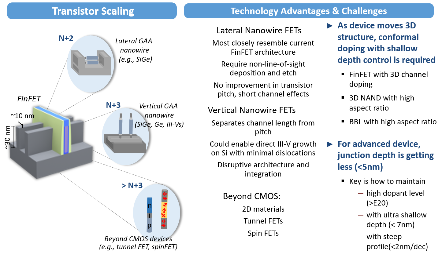
Ultra-Shallow Surface Modification
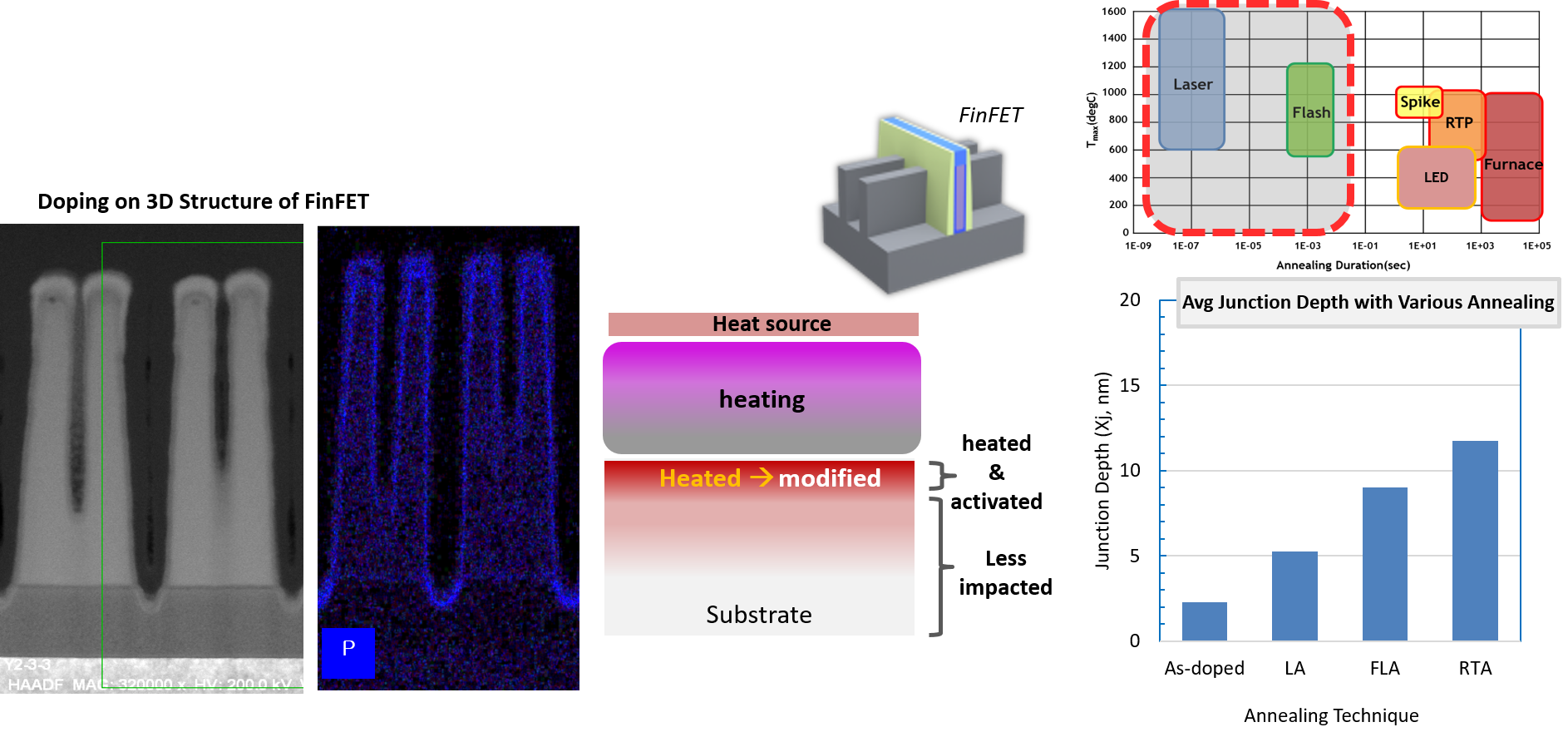
- Next generation semiconductor process (e.g. site-selective laser doping, solid diffusion, etching, deposition, and annealing) through short pulsed light sources.
- No structural damage or loss of 3D FinFET structure is seen after doping process.
- Shallowest junction depth (Xj) can be produced by laser process.Generated heat distribution after laser activation process is estimated through a thermal analysis.
*Research project & funding source:
“Characterization on the wafer surface for the advanced thermal pulsed process," funded by Lam Research Corp., USA
2016.02~2017.08
CTD,
Lam Research, Fremont, CA USA
Process Engineer
Next Generation Semiconductor Process Through Intense Light Sources
- Next generation semiconductor process (e.g. site-selective laser doping, solid diffusion, etching, deposition, and annealing) through short pulsed light sources.
- Thermal analysis for short pulsed heat sources and design of measuring temperature for pulsed heat sources.
Electrical Contact Resistance Improvement
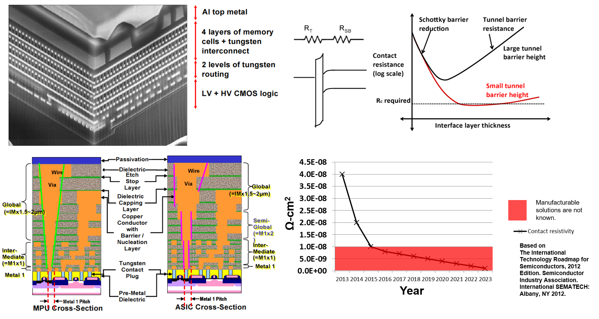
- Contact resistivity must be reduced to meet parasitic resistance requirements.
- Contact resistance increases inversely as square of contact size.

2011.08~2016.01
Laser Thermal Lab., UC Berkeley, Berkeley, CA USA
Graduate Student Researcher (Ph.D. course)/ Postdoctoral Fellow
Site Selective Laser Annealing for Flexible and Wearable Electronics with 2D Materials
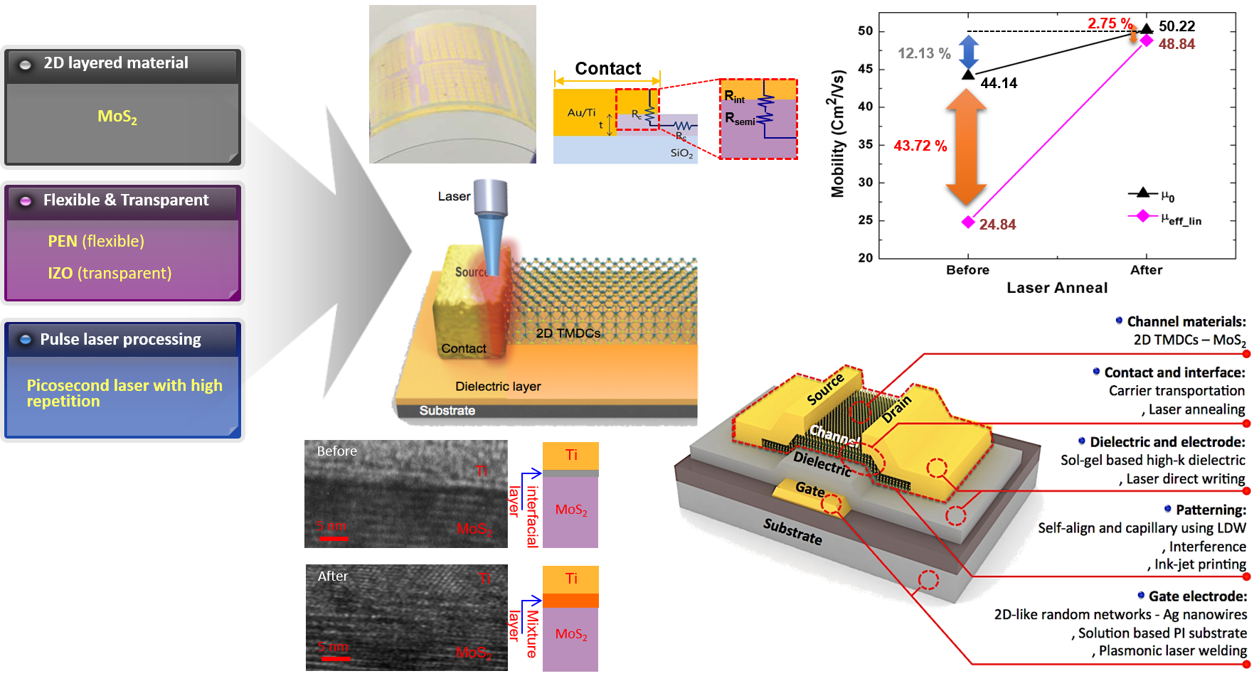
- Selective picosecond laser annealing of electrode contacts achieved enhanced electrical performance without damaging plastic substrate.
- Thermal analysis, electrical measurement, TEM images, and YFM enable understanding of the effects of pulsed laser annealing process.
Laser Welded 2D-Like Random Networks
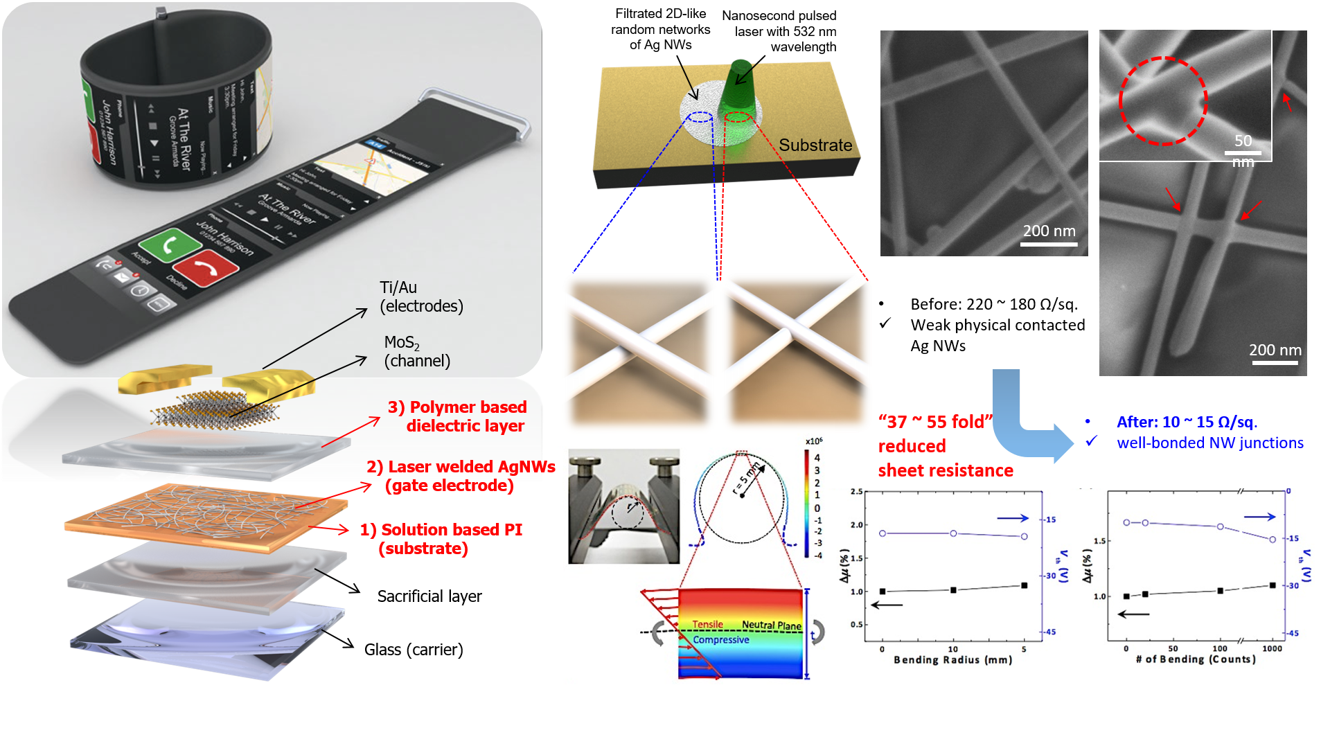
- Laser is applied to the welding for fabricating mechanically robust and electrically attractive 2D-like random networks.
- Plasmonic laser welding for mechanically flexible MoS2 transistors shows highly bending stability.
Laser Direct Writing (LDW) with Solution Based Materials & Ink-Jet Printing Process
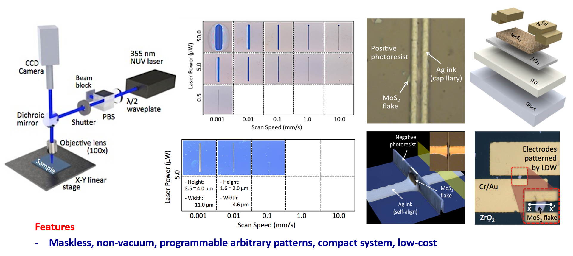
- Through laser direct writing (LDW) method, arbitrary fine patterns are produced for the electrodes as well as defining the channel of TFTs.
- LDW allows controlling the geometry of windows for lift-off processed metal electrodes with the small feature size (~ 1 μm), which is hard to create through the conventional photolithography process.
- Sol-gel processed metal oxide high-k ZrO2 is possible to form high quality metal oxide insulator without using the costly conventional vacuum processes based on the deposition tools and to deliver boosted the field effect mobility.

2009.02~2011.03
Display Lab., Samsung Advanced Institute of Technology (SAIT), Yongin, S. Korea
R&D Staff
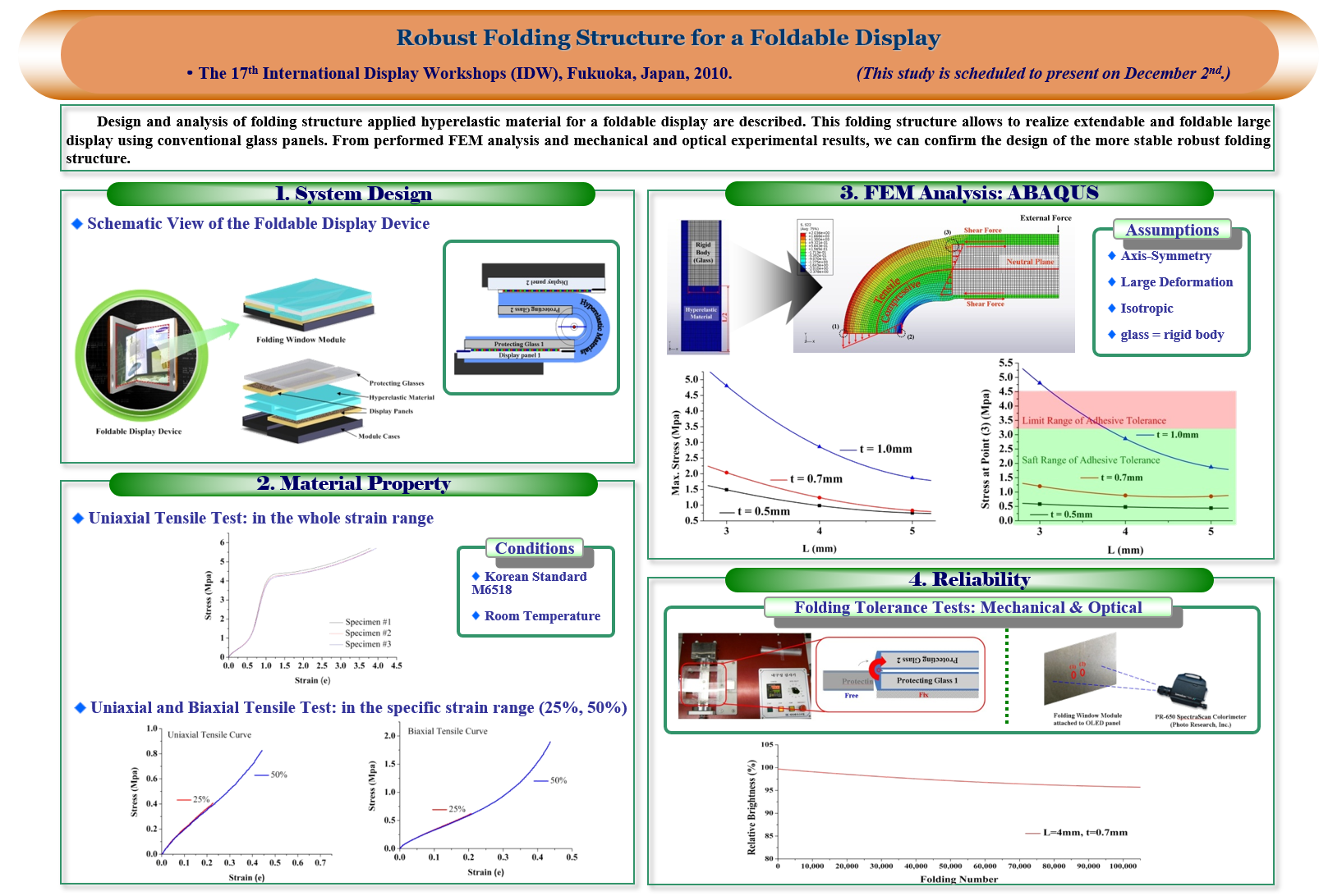
Seamless Foldable Display with AMOLED and Hyperelastic Materials
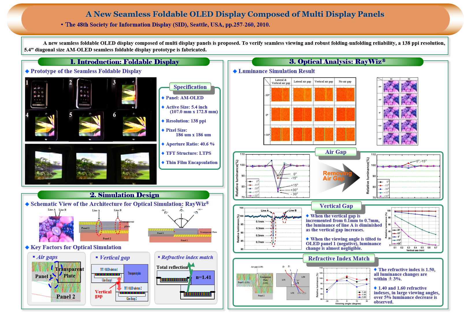
- A new seamless foldable OLED display composed of multi display panels is proposed.
- To verify seamless viewing and robust folding-unfolding reliability, a 138 ppi resolution, 5.4” diagonal size AMOLED seamless foldable display prototype is fabricated.
- From performed FEM analysis and mechanical and optical experimental results, we can confirm the design of the more stable robust folding structure.
Low Temperature Color Filter for Flexible AMOLED
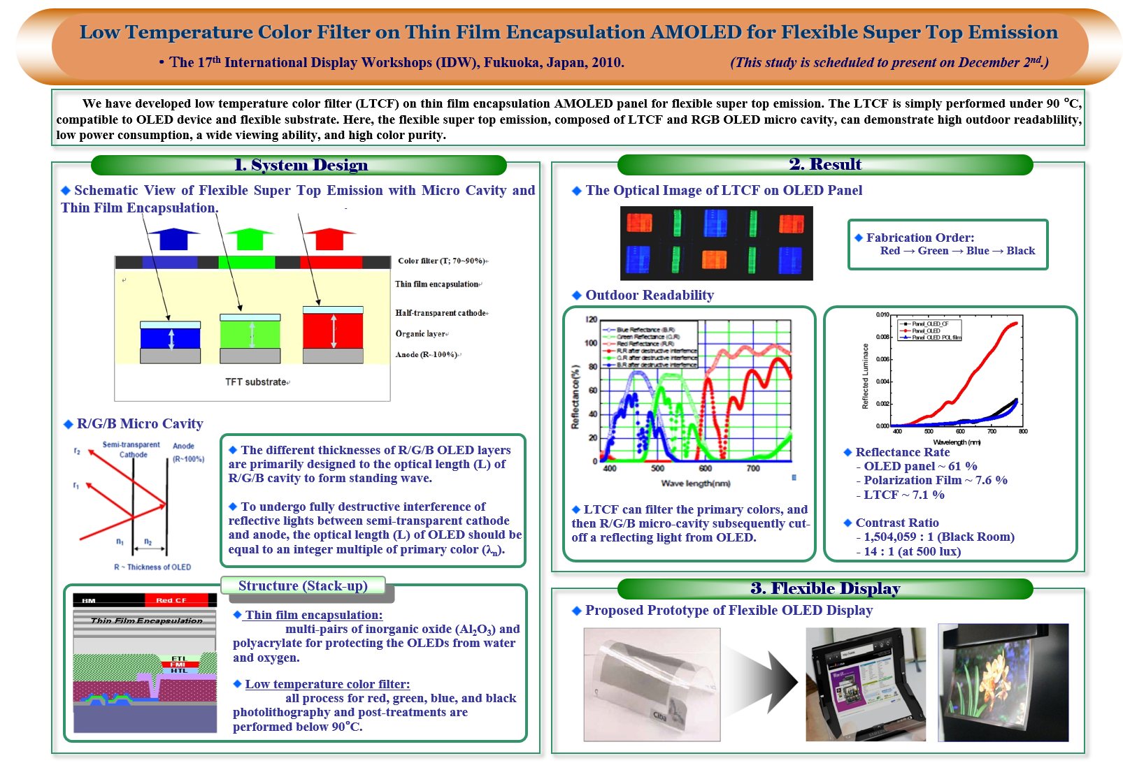
- We have developed low temperature color filter (LTCF) on thin film encapsulation AMOLED panel for flexible super top emission.
- The LTCF is simply performed under 90 °C, compatible to OLED device and flexible substrate.
- The flexible super top emission, composed of LTCF and RGB OLED micro cavity, can demonstrate high outdoor readablility, low power consumption, a wide viewing ability, and high color purity.
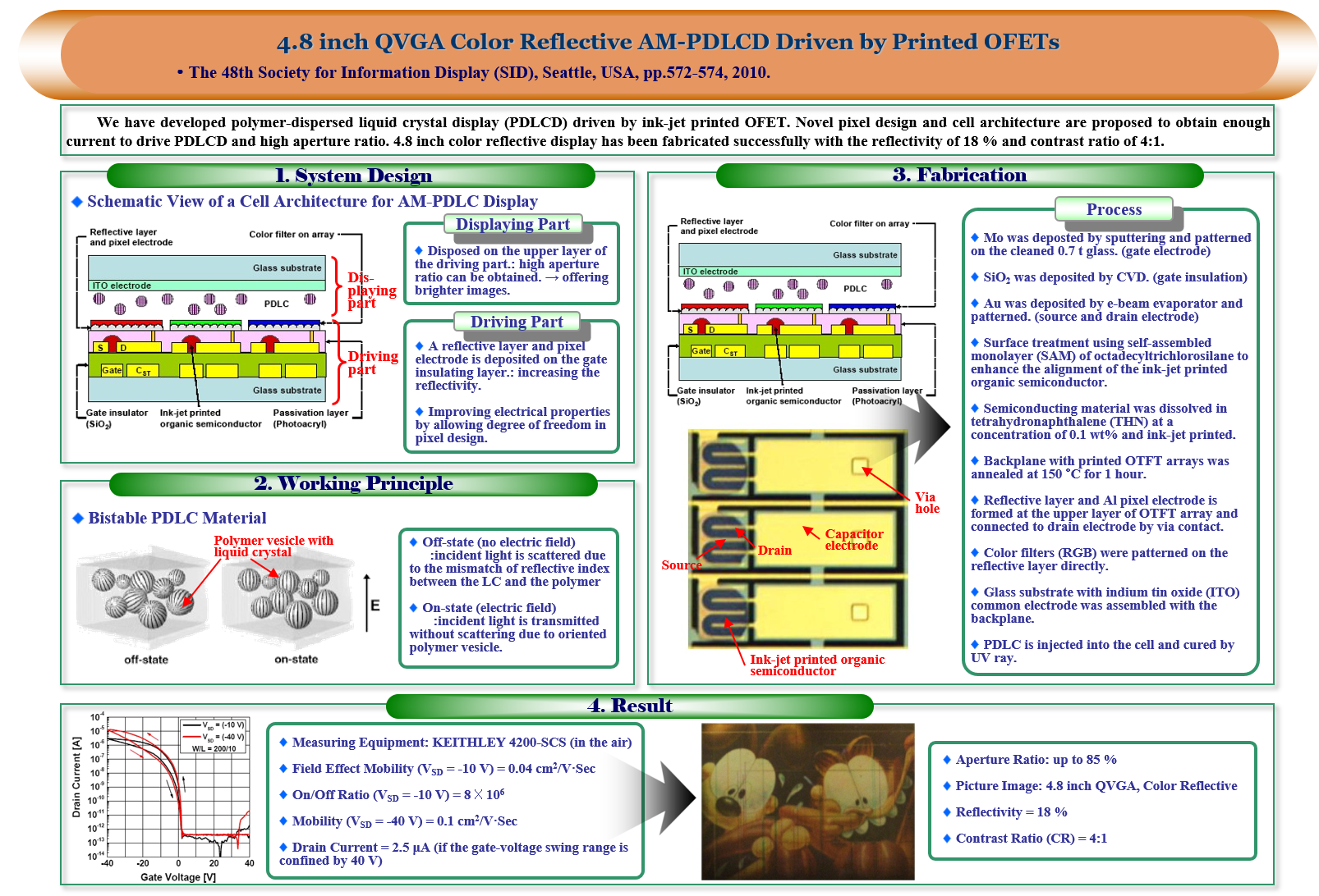
Reflective Displays: Electro-Chromic Display (ECD) & Polymer-Dispersed Liquid Crystal Display (PDLCD)
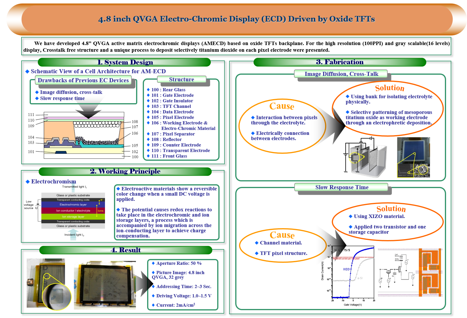
- We have developed 4.8” QVGA active matrix electrochromic displays (AMECD) based on oxide TFTs backplane.
- Also, We have developed polymer-dispersed liquid crystal display (PDLCD) driven by ink-jet printed OFET.
- Novel pixel design and cell architecture are proposed to obtain enough current to drive PDLCD and high aperture ratio.
Low Power MEMS Display
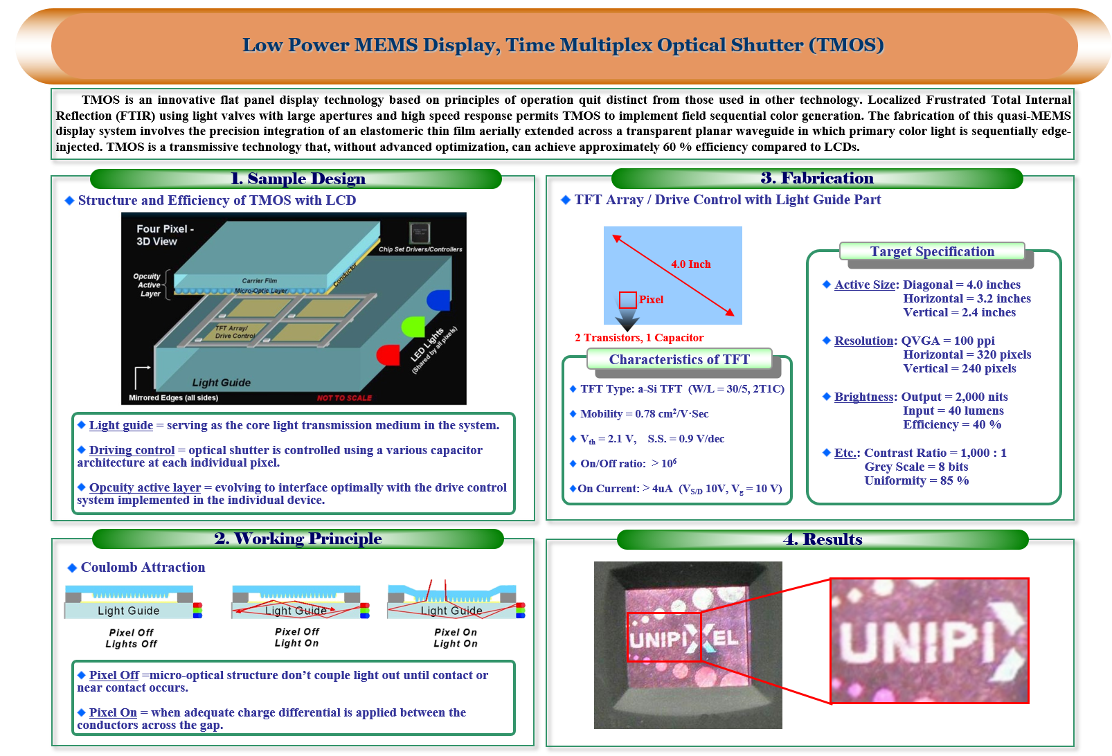
- Localized Frustrated Total Internal Reflection (FTIR) using light valves with large apertures and high speed response permits TMOS to implement field sequential color generation.
- The fabrication of this quasi-MEMS display system involves the precision integration of an elastomeric thin film aerially extended across a transparent planar waveguide in which primary color light is sequentially edge-injected.

2007.03~2009.02
Korea Advanced Institute of Science and Technology (KAIST), Daejeon, S. Korea
Graduate Student Researcher (Master course)
Haptic Devices (1): Braille Code Display
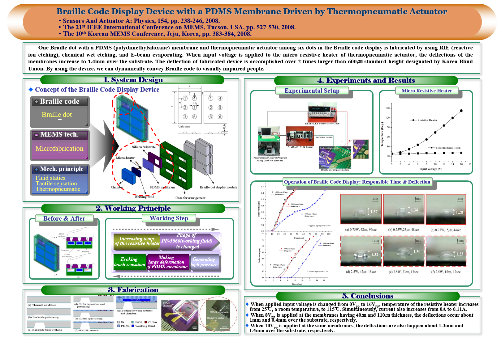
- One Braille dot with a PDMS (polydimethylsiloxane) membrane and thermopneumatic actuator among six dots in the Braille code display is fabricated.
- When input voltage is applied to the micro resistive heater of thermopneumatic actuator, the deflections of the membranes increase to 1.4mm over the substrate.
- By using the device, we can dynamically convey Braille code to visually impaired people.
Haptic Devices (2): Tunable Stiffness Display
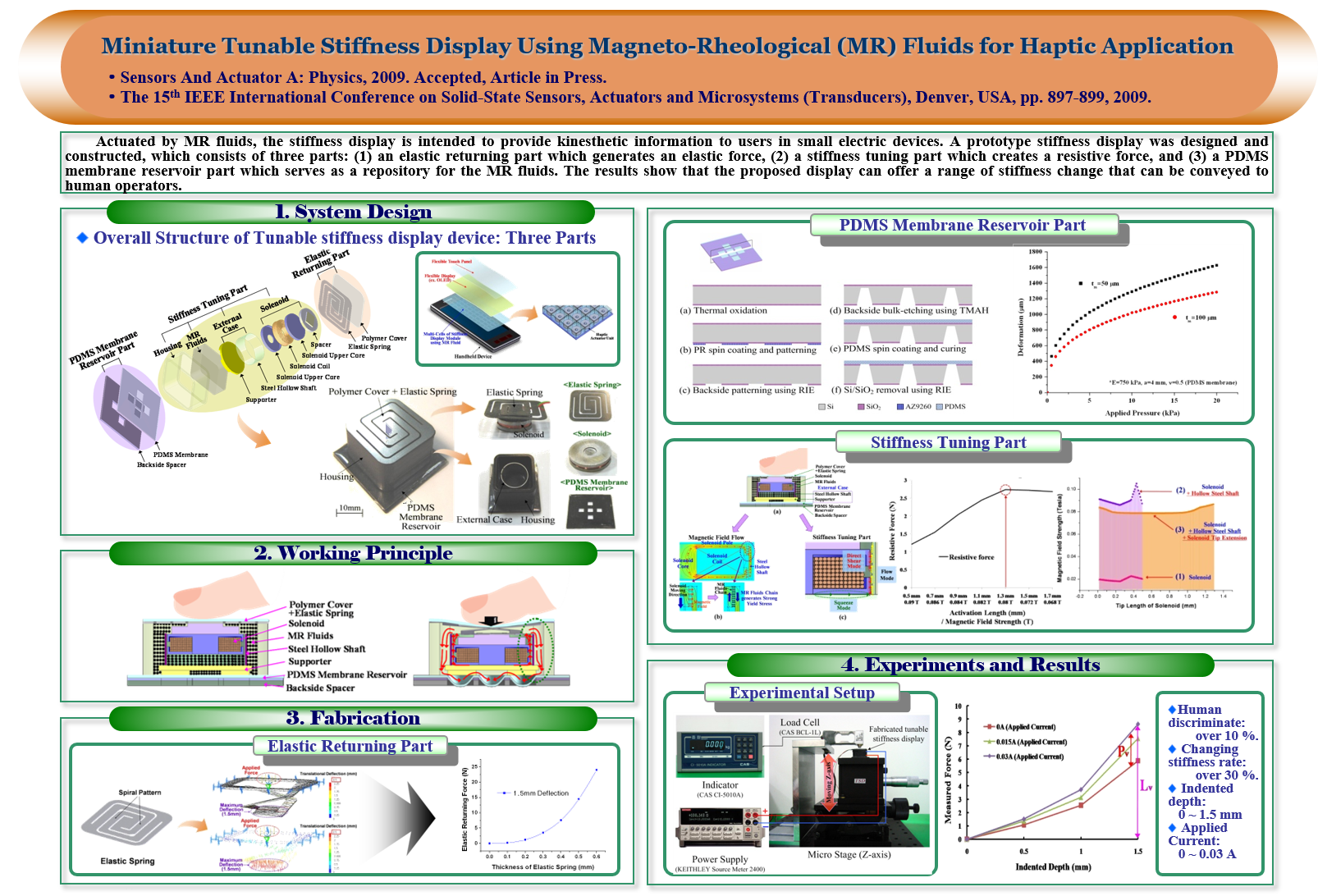
- Actuated by Magneto-Rheological (MR) fluids, the stiffness display is intended to provide kinesthetic information to users in small electric devices.
- The proposed devices can offer a range of stiffness change that can be conveyed to human operators.
Thermal Frequency Tuned Microactuator
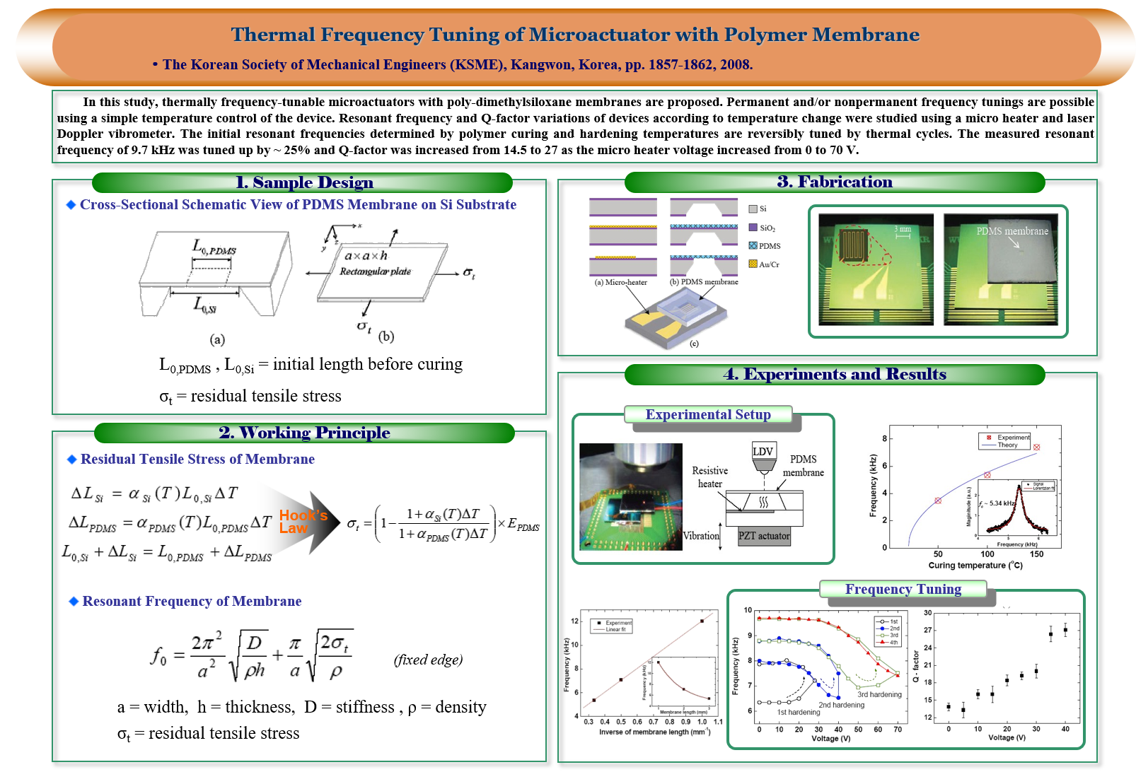
- Permanent and/or nonpermanent frequency tunings are possible using a simple temperature control of the device.
- The initial resonant frequencies determined by polymer curing and hardening temperatures are reversibly tuned by thermal cycles.